Ultimate Microscopy.
By: Steve Adams. G0KVZ
As presented to the Vange Amateur Radio Society 21st Jun 2007
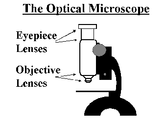 For the last 400 years, microscopes have been around in one form or another.
Although the actual inventor is unknown,
they were developed in the Netherlands between 1590 and 1608.
The lenses used in early examples were inadequate and resulted in rather poor images,
but even these early devices were a boon to scientists in their research into living
organisms.
For the last 400 years, microscopes have been around in one form or another.
Although the actual inventor is unknown,
they were developed in the Netherlands between 1590 and 1608.
The lenses used in early examples were inadequate and resulted in rather poor images,
but even these early devices were a boon to scientists in their research into living
organisms.
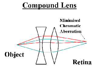 A compound lens is utilised in all modern microscopes as it is necessary to overcome
Chromatic Aberration.
A compound lens is utilised in all modern microscopes as it is necessary to overcome
Chromatic Aberration.
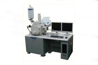 Development of the Electron microscope began in 1931, the first prototype,
capable of magnifying objects at just x400, was built by two German engineers,
Max Knoll and Ernst Ruska with the design being based on the work of Louis de Broglie,
a French physicist. Although Siemens held the patent (1931) it wasn't until 1937 that
they became actively involved by further developing the Electron microscope.
Modern electron microscopes are capable of magnifications of over x10,000
Development of the Electron microscope began in 1931, the first prototype,
capable of magnifying objects at just x400, was built by two German engineers,
Max Knoll and Ernst Ruska with the design being based on the work of Louis de Broglie,
a French physicist. Although Siemens held the patent (1931) it wasn't until 1937 that
they became actively involved by further developing the Electron microscope.
Modern electron microscopes are capable of magnifications of over x10,000
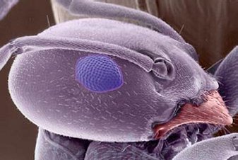
 The performance of an ordinary microscope it limited by the fact that light waves are relatively
large when compared to some of the objects that need to be viewed.
In fact, light would simply pass by a virus particle rendering it invisible to light.
The electron microscope isn't troubled by this limitation, as it utilises an electron beam.
This beam of electrons is accelerated to a very high velocity using very high voltages,
and is focused using magnetic and or electric fields.
The electrons interact with the sample,
and this interaction is sensed electronically and converted into an image.
The performance of an ordinary microscope it limited by the fact that light waves are relatively
large when compared to some of the objects that need to be viewed.
In fact, light would simply pass by a virus particle rendering it invisible to light.
The electron microscope isn't troubled by this limitation, as it utilises an electron beam.
This beam of electrons is accelerated to a very high velocity using very high voltages,
and is focused using magnetic and or electric fields.
The electrons interact with the sample,
and this interaction is sensed electronically and converted into an image.
 Surface features of an object - Hardness, reflectivity, etc.
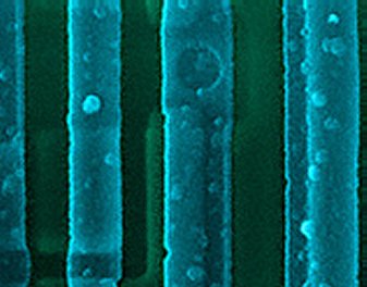 As mentioned previously, Electron microscopes can be used to show the internal fabrication of integrated circuits,
This is a fascinating topic, and there is a superb website devoted to the fantastic images of i.c's.
On these images examples can be seen of the hardware designers demonstrating how they can 'tag' their projects
in a way that would normally be invisible.
These 'doodlings' can be both ingenious and humourous.
As mentioned previously, Electron microscopes can be used to show the internal fabrication of integrated circuits,
This is a fascinating topic, and there is a superb website devoted to the fantastic images of i.c's.
On these images examples can be seen of the hardware designers demonstrating how they can 'tag' their projects
in a way that would normally be invisible.
These 'doodlings' can be both ingenious and humourous.